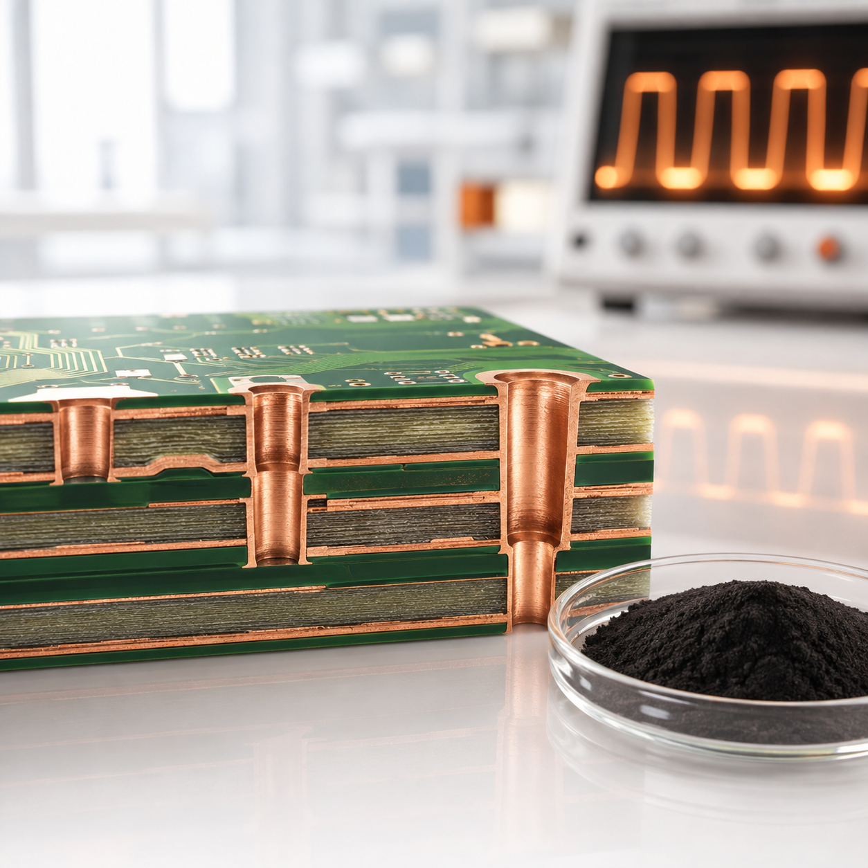
DC vs. Pulse Copper Plating for PCBs: Why Advanced Plating Lines Use Copper Oxide Replenishment
Published: 2026-09-08|Category: PCB Copper Plating Technology|Reading Time: 12 min
Key Takeaways
A blind via connects an outer layer to one or more inner layers without passing through the entire PCB. It is a key interconnect structure in HDI and other high-density boards.
Direct-current plating applies current continuously in one direction. It is a mature process used across a wide range of through-hole, pattern, and circuit plating applications.
Pulse plating controls the on-time, off-time, and, in pulse-reverse processes, the direction of current. This provides another way to manage ion transport and copper deposition.
With a properly matched waveform, bath chemistry, and equipment setup, pulse and pulse-reverse plating can improve blind-via filling and copper distribution in high-aspect-ratio through holes.
Pulse plating does not automatically require copper oxide. Copper oxide is primarily used as an external copper source in plating systems fitted with insoluble anodes.
Some advanced PCB lines combine pulse-reverse plating, dimensionally stable insoluble anodes, and automated copper oxide replenishment so that current waveform, anode geometry, and Cu²⁺ concentration can be controlled separately.
Electronic-grade copper oxide for an automated replenishment system must be evaluated for impurities, acid-insoluble matter, dissolution behavior, flowability, and lot-to-lot consistency.
Copper plating is one of the fundamental processes in PCB manufacturing.
Although the deposited copper layer is thin, it is responsible for electrical conduction, heat transfer, interlayer connection, and long-term reliability.
As PCB designs move toward HDI, higher layer counts, finer lines, smaller holes, and higher aspect ratios, copper plating has to meet a more demanding set of requirements:
deliver copper into smaller and deeper features;
reduce the difference between surface and in-hole copper thickness;
achieve complete and reliable blind-via filling;
minimize seams, dimples, and voids inside the via;
increase productivity without creating local burning or rough deposits;
keep copper-ion and additive concentrations stable; and
reduce particles, anode sludge, and manual maintenance.
This is why pulse plating, insoluble anodes, and copper oxide powder are increasingly discussed in relation to advanced PCB plating lines.
They are related, but they are not the same thing:
Pulse plating controls how current is delivered. The anode system determines how current enters the bath. Copper oxide provides a separate means of replenishing Cu²⁺.
Understanding these three functions helps explain why some HDI and high-aspect-ratio PCB lines combine pulse plating, insoluble anodes, and copper oxide replenishment.
Before comparing direct current with pulse current, it is useful to look at one of the PCB structures for which pulse plating is often considered: the blind via.
1. What Is a Blind Via in a PCB?
Holes in a PCB can be divided broadly into three groups:
Through holes pass through the entire board and can connect the top layer, bottom layer, and selected inner layers.
Blind vias begin at an outer surface and connect to one or more inner layers without passing through the whole board.
Buried vias are located entirely inside the PCB and connect inner layers only, so they are not visible from either outer surface.
Blind vias create interlayer connections while using less routing space than holes that pass through the entire board.
They are widely used in HDI boards for smartphones, servers, automotive electronics, communications equipment, and other high-density products.
As electronic products become smaller and component I/O density rises, PCB designers have to fit more connections into a limited area. Blind vias are one of the structures that make this higher interconnection density possible.
2. Why Is Blind-Via Copper Plating More Difficult Than Plating a Flat Surface?
Blind vias improve routing density, but they also create a more difficult plating environment.
On an open panel surface, the plating solution can circulate freely, allowing Cu²⁺ and organic additives to reach the cathode relatively easily.
A blind via is a confined feature with only one open end. The solution must enter through the via mouth, while copper ions must continue to move toward the bottom of the feature.
Without effective process control, copper often deposits faster at the panel surface and via mouth than at the bottom. These areas are closer to the bulk solution and may experience stronger Cu²⁺ transport and higher local current density.
If the via mouth builds up too quickly, the opening can narrow before the lower part of the via has been filled. Possible defects include:
insufficient deposition at the via bottom;
surface dimples;
uneven copper thickness;
seams or internal voids;
premature closure at the via mouth; and
reduced interconnection reliability after thermal cycling.
The objective of blind-via plating is therefore not simply to coat the sidewall with copper. Depending on the board design, the process must achieve uniform deposition or controlled bottom-up filling.
An idealized blind-via filling sequence can be understood as:
Faster deposition at the bottom
↓
Controlled upward growth of copper
↓
Fewer seams and voids
↓
A relatively level plated surface
This process is commonly known as blind-via filling or microvia filling.
3. What Determines Blind-Via Filling Performance?
Good blind-via filling is not determined by current density alone.
The result depends on a combination of factors:
via diameter and depth;
via aspect ratio;
preparation and metallization of the via bottom and sidewall;
Cu²⁺ and sulfuric-acid concentrations;
the balance of accelerator, leveler, and suppressor additives;
solution circulation, impingement flow, and panel movement;
current density and plating time;
DC, pulse, or pulse-reverse waveform;
anode design and anode-to-cathode spacing; and
the rate and stability of copper replenishment.
Additives selectively influence deposition at the surface, via mouth, and via bottom. Fluid delivery moves Cu²⁺ and additives into the feature, while the waveform controls the timing of copper deposition.
Blind-via filling is therefore a system-level process involving the PCB structure, bath chemistry, power waveform, anode design, and plating equipment.
This leads to the central question of this article:
As blind vias become smaller and PCB structures become more complex, what changes when continuous DC is replaced by a controlled pulse waveform?
4. What Is DC Copper Plating?
What is sometimes called “conventional-current plating” is more accurately described as direct-current, or DC, plating.
During DC copper plating, current flows continuously in the same direction. Cu²⁺ in the bath gains electrons at the PCB surface and is deposited as metallic copper:
Cu²⁺ + 2e⁻ → Cu
When the line uses soluble phosphorized-copper anodes, metallic copper dissolves at the anode at the same time:
Cu → Cu²⁺ + 2e⁻
Phosphorized copper balls in a conventional DC system therefore perform two functions:
They act as the anode and carry current into the bath.
They dissolve to replenish the Cu²⁺ consumed during plating.
DC plating is mature, comparatively straightforward to operate, and supported by well-established equipment, chemistry, additive, and process-control practices.
For many through-hole, pattern-plating, and circuit-plating applications, it remains an efficient and dependable choice.
5. The Mass-Transport Challenge in DC Plating
As copper deposits on the PCB, Cu²⁺ is consumed near the cathode surface.
On an open panel surface with good solution movement, those ions can usually be replenished relatively quickly. In deep holes, small vias, and the bottom of blind vias, solution exchange and ion diffusion are more restricted.
If Cu²⁺ is consumed faster than it can be transported back to the interface, the local copper-ion concentration falls.
At the same time, the panel surface and via mouth tend to receive current more readily and may plate faster than recessed areas.
This can result in:
thicker copper on the panel and thinner copper in the hole;
rapid buildup at the via mouth, further restricting solution exchange;
lower throwing power in high-aspect-ratio through holes;
incomplete filling, dimples, or voids in blind vias; and
roughness or burning at high-current-density areas when the plating rate is increased.
Circulation, impingement flow, shielding, rectifier settings, and additives can all improve the result. Continuous DC, however, provides less flexibility for controlling deposition over time.
6. What Is Pulse Copper Plating?
Pulse plating does not apply one constant current continuously. Instead, it alternates between current-on and current-off periods according to a defined cycle.
A simplified pulse cycle looks like this:
Forward current → Off-time → Forward current → Off-time
During the forward pulse, Cu²⁺ gains electrons and deposits as metallic copper on the PCB.
During the off-time, deposition pauses while copper ions continue to diffuse toward the cathode surface and into recessed features.
This interval gives the local Cu²⁺ concentration time to recover and can help reduce concentration polarization.
Controllable pulse-plating parameters include:
peak current density;
average current density;
on-time;
off-time;
pulse frequency;
duty cycle; and
waveform shape within each cycle.
Compared with DC plating, pulse plating adds a further level of control:
The process engineer can manage not only how much current is applied, but also when and for how long it is applied.
7. What Is Pulse-Reverse Copper Plating?
Pulse-reverse plating, also called reverse-pulse plating or periodic pulse reverse plating, introduces a short reverse-current step between forward deposition periods:
Forward deposition → Brief reverse pulse → Forward deposition
The forward step is responsible for most of the copper deposition.
The reverse step briefly acts on the copper that has already been deposited. Because the panel surface and via mouth are typically higher-current-density areas, the reverse pulse may affect those locations more strongly.
When the waveform, bath chemistry, additives, and equipment are properly matched, this can help to:
limit excessive buildup on the panel and at the via mouth;
improve current distribution into recessed features;
reduce the difference between surface and in-hole copper thickness;
improve throwing power in high-aspect-ratio through holes;
support blind-via filling; and
maintain deposit quality at higher production current.
Pulse reverse is not simply a matter of switching the current backward for a moment.
An unsuitable waveform can reduce plating efficiency, complicate additive control, or affect deposit properties. The pulse program must be developed together with the bath formulation, additive package, fluid delivery, and PCB geometry.
8. DC vs. Pulse Copper Plating
ComparisonDC Copper PlatingPulse or Pulse-Reverse Copper PlatingCurrent deliveryContinuous and unidirectionalAlternates between on/off periods or forward/reverse currentMain parametersCurrent density and plating timePeak current, frequency, duty cycle, and forward/reverse durationCopper-ion transportRelies mainly on diffusion and solution movementOff-time provides an additional interval for concentration recoveryDistribution controlManaged mainly through equipment, shielding, flow, and additivesThe waveform provides another way to control depositionThrough-hole and via performanceSuitable for a wide range of conventional PCB applicationsCan provide advantages for complex features when correctly configuredPower supplyComparatively simpleRequires a more capable rectifier and control systemProcess setupMature and relatively directRequires coordinated optimization of waveform, chemistry, and equipmentProduction managementFewer electrical variablesMore control variables and greater demand for process records
It is therefore too simplistic to say that pulse plating is always better than DC plating.
A more useful conclusion is:
DC plating is a mature and stable choice for high-volume conventional production, while pulse plating gives process engineers more options for managing copper deposition in complex PCB structures.
9. Why Do Advanced PCBs Place More Emphasis on Pulse Plating?
“Advanced PCB” is not one single product category.
HDI boards, IC substrates, high-layer-count boards, and high-frequency or high-speed PCBs have different requirements. They do, however, share several design trends:
smaller hole diameters;
more complex stackups;
higher through-hole aspect ratios;
greater use of blind, stacked, and via-in-pad structures;
finer lines and spaces; and
tighter requirements for copper uniformity and interconnection reliability.
For these structures, the objective is no longer simply to deposit copper. The process must control where copper deposits first, how quickly it grows, and how deposition is balanced between the board surface and recessed features.
The time-domain control provided by pulse and pulse-reverse plating can work together with:
copper and sulfuric-acid concentrations;
leveler, accelerator, and suppressor additives;
circulation and impingement flow;
anode-to-cathode spacing;
panel movement; and
online analysis and automatic dosing.
This is why pulse plating is often considered for HDI blind-via filling and high-aspect-ratio through-hole plating.
It remains only one part of the process. Poor hole preparation, weak solution exchange, an additive imbalance, or unstable Cu²⁺ concentration cannot be corrected simply by installing a pulse rectifier.
10. Why Is Pulse Plating Often Paired with Insoluble Anodes?
Two separate concepts must be distinguished:
pulse plating is a method of delivering electrical current;
an insoluble anode is a type of anode system.
Pulse plating can operate with soluble phosphorized-copper anodes or insoluble anodes. DC plating can also be configured with either anode type.
When a production line targets higher current density, more repeatable in-hole distribution, and a greater level of automation, however, the fixed geometry of an insoluble anode can provide useful process advantages.
Phosphorized copper balls become smaller as they dissolve. Their effective area, packing condition in the anode basket, and relationship to the cathode may change over time.
An insoluble anode is typically based on titanium with a mixed-metal-oxide coating. Under normal operating conditions, it is not intended to dissolve as the copper source, so its dimensions and position remain comparatively stable.
This fixed structure can help a line to:
maintain more consistent anode-to-cathode spacing;
reduce changes in the electric field caused by anode consumption;
design current distribution around the tank and panel geometry;
reduce copper-ball loading and basket maintenance;
lower the burden associated with anode sludge and copper fines; and
integrate the anode system with continuous, automated plating equipment.
Some advanced lines therefore select insoluble anodes not because phosphorized copper is incompatible with pulse plating, but because fixed anode geometry removes one changing variable from the process.
11. Why Does an Insoluble-Anode System Need Copper Oxide Replenishment?
As copper is deposited at the cathode, Cu²⁺ is continuously removed from the plating solution.
A soluble phosphorized-copper anode replaces Cu²⁺ through anodic dissolution. An insoluble anode does not supply enough copper ions in this way.
Without an external copper source, the Cu²⁺ concentration in the bath would continue to fall.
An insoluble-anode line must therefore include a separate copper-replenishment system. Available approaches include:
copper oxide powder;
copper sulfate or another suitable copper salt;
an external metallic-copper dissolution unit using an Fe²⁺/Fe³⁺ redox system; and
other validated external copper-dissolution technologies.
In other words, an insoluble anode does not automatically mean that copper oxide is the only possible replenishment material.
Copper oxide is widely considered because it reacts in a sulfuric-acid medium to form the Cu²⁺ required by the bath:
CuO + H₂SO₄ → CuSO₄ + H₂O
Replenishment can take place in a separate, controlled unit:
Metered copper oxide feed
↓
Reaction with an acidic solution
↓
Filtration of undissolved particles
↓
Copper concentration measurement or control
↓
Transfer of copper-containing solution to the production bath
The design separates current delivery from copper replenishment:
the insoluble anode establishes the electric field;
the pulse rectifier controls the deposition waveform; and
the copper oxide system maintains the Cu²⁺ concentration.
12. What Does the Combination of Pulse Plating and Copper Oxide Achieve?
The value of the system lies not in one isolated specification, but in its ability to control several production variables separately.
1. Independent Waveform Optimization
The forward, off-time, and reverse portions of the waveform can be adjusted for the PCB geometry and plating objective without relying on anode dissolution to manage copper replenishment.
2. More Stable Anode Geometry
An insoluble anode does not continually shrink like a consumable copper ball, helping to maintain its position, effective area, and spacing from the cathode.
3. Independent Copper-Concentration Control
Copper oxide can be metered according to accumulated ampere-hours, online analytical results, or production load.
As copper deposition increases, the replenishment unit can raise the rate at which copper oxide is dissolved and returned to the line, helping to limit large changes in bath Cu²⁺ concentration.
4. Better Suitability for Automation
Copper oxide storage, metering, dissolution, filtration, and transfer can be integrated into a dedicated automated module, reducing variation from manual addition.
The control system can also record:
copper oxide feed quantity;
accumulated ampere-hours;
dissolution time;
copper-ion concentration;
filtration status;
replenishment timing; and
equipment alarms and exceptions.
These records support process repeatability and traceability.
5. Fewer Anode-Generated Particles
Eliminating continuously dissolving copper balls can reduce the particle-management burden associated with anode film, copper fines, and anode sludge.
It does not eliminate particle control from the process. Acid-insoluble matter in the copper oxide, dissolution completeness, and filtration performance still require close attention.
6. Better Alignment Between Copper Replenishment and Production Demand
During continuous plating, the PCB continuously removes Cu²⁺ from the solution.
If copper oxide dissolves too slowly, or if the replenishment rate cannot keep up with production, the Cu²⁺ concentration can still fall.
A copper oxide powder with stable activity and predictable bath-dissolution behavior therefore helps an automated system respond to copper consumption more effectively.
13. What New Controls Does This System Require?
Pulse plating with insoluble anodes and copper oxide replenishment is not simply a matter of replacing several pieces of conventional equipment with more advanced ones.
The system introduces its own requirements:
investment in pulse rectifiers and control systems;
development of the forward and reverse waveform;
management of insoluble-anode coating life;
control of additive oxidation associated with oxygen evolution at the anode;
automated copper oxide metering and dissolution equipment;
online Cu²⁺ analysis;
filtration of undissolved particles;
control of additive concentrations and breakdown products; and
equipment interlocks and production-data traceability.
If copper oxide dissolution is inconsistent, or if the practical replenishment rate cannot match copper deposition, Cu²⁺ can still fluctuate in the production bath.
If acid-insoluble matter and other particles in the copper oxide are not properly controlled, they may increase the load on the filtration system.
Advanced plating equipment therefore has to be supported by consistent raw materials, bath management, defined test methods, and reliable process control.
14. What Should Be Checked in Copper Oxide Used for Pulse-Plating Replenishment?
CuO content alone is not enough to qualify copper oxide powder for an insoluble-anode replenishment system.
The evaluation should also cover:
CuO content and lot-to-lot variation;
metallic impurities such as Fe, Zn, Ni, and Pb;
chloride content;
acid-insoluble matter;
sulfuric-acid dissolution time;
dissolution time in the actual or simulated plating bath;
particle size and powder flowability;
compatibility with automated metering equipment;
consistency across consecutive lots; and
COA documentation and production traceability.
Dissolution time must be understood in the context of its test method.
A sulfuric-acid test provides a rapid indication of basic CuO activity. An operating PCB bath, however, already contains Cu²⁺, organic additives, and other process constituents, so it does not provide the same dissolution environment as acid alone.
For an automated replenishment system, dissolution in a representative plating solution is often more relevant to production than a single acid-dissolution number.
Zhongan electronic-grade active copper oxide powder is made from electrolytic copper through a controlled ammonia-stripping process, followed by washing, calcination, screening, and automated process control.
Under defined test conditions:
dissolution in sulfuric acid is completed within 10 seconds;
the plating-bath dissolution specification is no more than 12 minutes;
a representative high-copper, low-acid bath result is approximately 10 minutes; and
a representative high-acid, low-copper bath result is approximately 4 minutes.
These results do more than indicate that the powder dissolves quickly. They help show whether an automated replenishment system can respond promptly to Cu²⁺ consumption while limiting undissolved material and delayed copper-concentration recovery.
Final performance and suitability should be confirmed against the delivered lot COA, the agreed test method, and validation in the customer’s own production system.
For a detailed comparison of acid and plating-bath dissolution, see Does Faster Always Mean Better? Acid Dissolution vs. Plating-Bath Dissolution of Copper Oxide Powder.
For more information on particle control, see Why Acid-Insoluble Matter and Particle Residue Matter in High-Density HDI PCB Copper Plating.
To understand how manufacturing affects powder structure and activity, see Why Use Ammonia-Stripping to Make Electronic-Grade Copper Oxide Powder?.
For guidance on COAs and supplier evaluation, see How to Choose Electronic-Grade Copper Oxide Powder for PCB Plating.
Conclusion
The difference between DC and pulse copper plating goes beyond whether the current is continuous.
DC plating uses a steady, unidirectional current. It is mature and remains well suited to a broad range of PCB products.
Pulse and pulse-reverse plating control the timing and direction of current, giving process engineers more options for managing copper deposition in HDI blind vias, high-aspect-ratio through holes, and other complex structures.
When an insoluble anode is added to the system, the anode geometry remains comparatively stable, but the bath can no longer rely on anodic copper dissolution to replenish Cu²⁺.
Copper oxide is one option for supplying that copper externally.
The process logic behind pulse plating, insoluble anodes, and copper oxide replenishment is therefore straightforward:
The pulse rectifier controls how copper deposits. The fixed anode controls how the electric field is distributed. The copper oxide system controls how Cu²⁺ is replenished.
This separation of functions provides more process-control options for HDI, high-aspect-ratio PCB structures, and automated continuous plating. It is not, however, the only valid configuration for every advanced PCB line.
The final choice must reflect board geometry, equipment design, bath chemistry, capacity requirements, and quality targets.
The best solution is not determined by one power supply, one anode, or one replenishment material. It is the system that brings waveform control, anode geometry, bath management, and copper replenishment together in a stable, verifiable, and traceable process.
FAQ
What is a blind via in a PCB?
A blind via begins at an outer PCB surface and connects to one or more inner layers without passing through the entire board. It provides compact interlayer connections and is commonly used in HDI designs.
What is the difference between a blind via and a through hole?
A through hole passes through the entire PCB and can connect the top, bottom, and selected inner layers. A blind via connects an outer surface to only part of the layer stack.
Why can voids form during blind-via plating?
A blind via has only one open end, so solution exchange and Cu²⁺ transport are more difficult than on a flat surface. If copper builds up too quickly at the via mouth, it may narrow or close before the bottom is filled, leaving a seam or void.
Is pulse copper plating always better than DC plating?
No. DC plating is mature and effective for many conventional PCB products. Pulse plating offers additional control for complex features, but it also requires more capable equipment and more demanding process optimization.
Does pulse plating always require copper oxide powder?
No. Pulse describes the electrical waveform, while copper oxide is a replenishment material. A pulse-plating line with soluble phosphorized-copper anodes can replenish Cu²⁺ through anodic dissolution.
Why does an insoluble anode require a separate copper source?
An insoluble anode carries current but does not continuously release enough Cu²⁺ to replace the copper deposited on the PCB. The line therefore needs copper oxide, an external copper-dissolution unit, or another suitable replenishment source.
Why is pulse-reverse plating used for HDI blind vias?
With a properly developed process, the off-time and brief reverse steps can influence deposition at the panel surface, via mouth, and via bottom differently, helping to improve via filling and copper distribution.
Can copper oxide powder be added directly to the production plating tank?
It is normally metered, dissolved, and filtered in dedicated equipment before the copper-containing solution is returned to the production bath. Unvalidated direct addition of powder to the main tank is generally not recommended. The exact method should follow the plating-equipment and chemistry supplier’s process requirements.
What is the difference between sulfuric-acid dissolution and plating-bath dissolution?
A sulfuric-acid test measures basic powder activity. A working bath already contains Cu²⁺ and organic additives and provides a more complex dissolution environment, so a plating-bath test is generally more representative of production.
How can a buyer determine whether copper oxide is suitable for an automated replenishment system?
The review should include CuO content, metallic impurities, chloride, acid-insoluble matter, acid- and bath-dissolution behavior, particle size, flowability, and lot consistency, followed by validation with the intended equipment and bath chemistry.
This article was prepared by the Zhongan Copper technical team.
Zhongan Copper develops and manufactures high-purity active copper oxide powder for electronic applications, including acid copper-plating systems used in PCB, FPC, and HDI production.
Contact our technical team to request product specifications, a lot COA, particle-size data, sulfuric-acid dissolution results, plating-bath dissolution data, or sample-validation support for an insoluble-anode replenishment system.
Final product specifications and application results are subject to the COA for the delivered lot, the agreed test method, and validation in the customer’s production process.