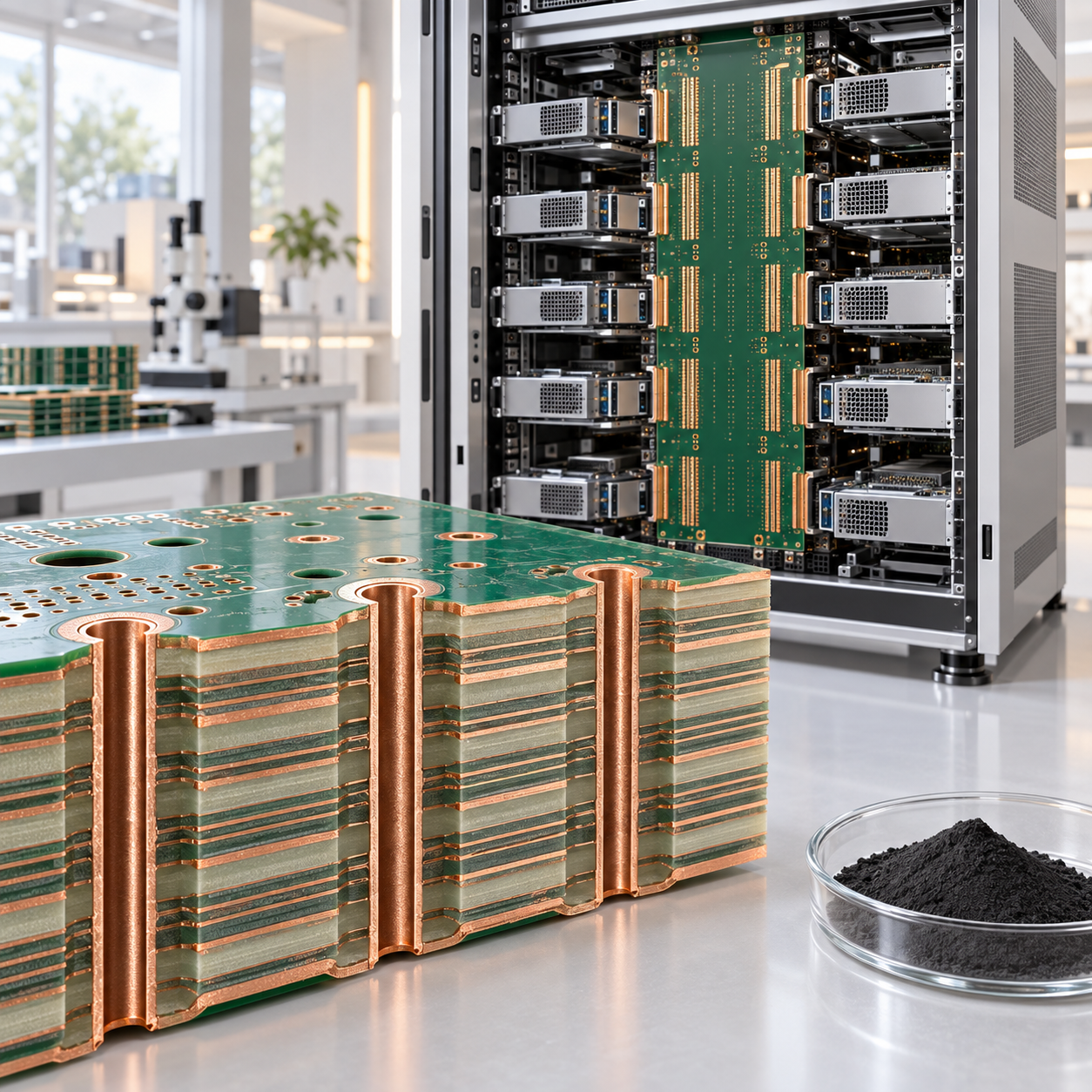
Why AI Servers Need High-Layer-Count PCBs: From Rubin Cableless Interconnects to High-Aspect-Ratio Through-Hole Plating
Published: 2026-09-13|Category: AI Servers and PCB Copper Plating|Reading Time: 15 min
Key Takeaways
Progress in AI servers depends on more than GPU performance. High-speed interconnects, power delivery, cooling, and rack architecture are equally important at system level.
New rack-scale systems are using PCB midplanes and backplanes for some internal high-speed connections, reducing the dependence on conventional copper cabling and shortening signal paths.
As more high-speed signal, power, and ground functions move onto the PCB, boards may become larger, thicker, higher in layer count, and more complex in construction.
When board thickness increases while finished hole diameter remains small, the aspect ratio of plated through holes rises.
High-aspect-ratio holes are more difficult to plate uniformly and are more likely to show thin copper at the hole center and excessive buildup near the hole openings.
Pulse current, solution flow, additives, and stable Cu²⁺ replenishment must work together. No single parameter can solve every deep-hole plating challenge.
In an insoluble-anode system, electronic-grade copper oxide can serve as an external copper source. Its impurities, acid-insoluble matter, and dissolution behavior can affect replenishment stability.
When people discuss AI servers, the conversation usually begins with GPU count, computing power, and model-training speed.
Once dozens of GPUs, CPUs, switching devices, and network components are installed in the same rack, however, chip performance is only part of the system-level challenge.
The overall system also depends on how quickly those processors exchange data, how reliably power is delivered, how effectively heat is removed, and how consistently a large number of computing modules remain connected.
For this reason, the development of AI servers is moving beyond the upgrade of individual server boards toward coordinated rack-scale design.
This shift is also changing the role of the printed circuit board.
A PCB is no longer only a platform for mounting electronic components. In some advanced systems, it is becoming a system-level interconnect platform that links compute trays, switch trays, power modules, and control systems.
That raises an important manufacturing question:
As AI-server PCBs become larger, thicker, and higher in layer count, what new challenges arise in plated through-hole copper deposition?
1. AI Server Progress Is About More Than GPUs
An AI server has to perform a large amount of parallel computation.
If each GPU is viewed as one compute unit, the system still needs a high-bandwidth, low-latency network that allows many GPUs to exchange data continuously.
As GPU count and compute scale increase, the rack must handle several functions at the same time:
high-speed GPU-to-GPU communication;
data transfer between GPUs and switching devices;
CPU-to-GPU connectivity;
network, storage, and control signals;
high-current power delivery;
liquid cooling or other thermal-management systems; and
equipment monitoring and fault management.
If every module is connected by large numbers of individual copper cables, the rack can become crowded and difficult to assemble, route, and maintain.
AI-server architecture is therefore advancing not only through faster chips, but also through new approaches to internal rack connectivity.
2. What Does “Cableless” Interconnection Mean in an AI Rack?
The term “cableless” does not mean that every cable disappears from an AI rack.
A more accurate description is:
Some internal connections previously carried by separate high-speed copper cables are transferred to PCB midplanes, backplanes, and connector systems.
In a conventional rack architecture, large numbers of high-speed copper cables may be needed between compute trays and switch trays.
As the number of connections grows, this approach can create several practical challenges:
cables occupy valuable rack space;
routing becomes more complex;
assembly work increases;
the number of connection points grows;
troubleshooting and replacement become more difficult;
cable bundles can interfere with airflow and cooling space; and
signal-path consistency becomes more difficult to manage.
With a PCB midplane or backplane, functional trays connect through board-mounted connectors, while high-speed signals travel through controlled PCB routing.
In its 2026 GTC presentation, NVIDIA showed compute nodes and a rack midplane associated with its next-generation Rubin architecture. The company explained that the midplane replaces some conventional copper-cable connections whose transmission distance had become a limiting factor.
The point of this design is not simply to remove a few cables. It is to redesign how compute modules, switching modules, and the rack connect as one system.
3. What Are a PCB Midplane and an Orthogonal Backplane?
PCB Midplane
A PCB midplane is positioned between different functional modules. Connectors on two sides or in different locations allow compute trays, switch trays, and other units to interface through the board.
Depending on the system, a midplane may carry more than high-speed data. It may also include:
power connections;
ground references;
management and control signals;
equipment-status monitoring;
module identification; and
auxiliary power functions.
Orthogonal Backplane
In an orthogonal interconnect architecture, modules approach an intermediate board or connector system from different directions, forming an approximately 90-degree connection.
For example:
compute trays may be inserted horizontally;
switch trays may be inserted vertically; and
the two sets of modules communicate through the intermediate backplane and connector system.
This arrangement can shorten selected signal paths, reduce separate cabling, and support a more modular rack architecture.
An orthogonal backplane is not a fixed design that can simply be applied to every AI server. The practical structure still depends on the processor platform, connector system, data rate, power architecture, cooling method, and equipment supplier’s design.
4. Why Does Cableless Interconnection Raise PCB Requirements?
When functions previously carried by separate copper cables move onto a PCB, that board must handle more signals and more system-level responsibilities.
It may need to satisfy several demanding requirements at once:
greater high-speed channel density;
more complex interlayer connections;
higher connector density;
tighter impedance control;
lower signal-transmission loss;
more stable power and ground networks;
greater connector-position accuracy;
stricter dimensional and warpage control; and
long-term reliability under repeated thermal cycling.
To accommodate high-speed signal layers, power planes, ground planes, and control routing, some AI-server PCBs may require higher layer counts and more complex stackups.
Industry analysis from TrendForce indicates that systems associated with the Rubin generation are driving demand for larger boards, higher layer counts, and more complex rack-level PCBs, including midplanes and orthogonal backplanes.
An important qualification must be made:
Final PCB layer count, board thickness, and hole structure should be based on the confirmed design from the equipment company and PCB manufacturer.
Some unofficial online materials publish very specific layer counts and dimensions. Without official drawings or supply-chain confirmation, those figures should not be treated as a standard mass-production specification.
5. What Is a High-Layer-Count PCB?
A high-layer-count PCB is not simply a conventional board with more layers added to it.
As the number of layers increases, the manufacturer has to manage a broader set of interacting challenges:
registration between circuit layers;
dimensional change during repeated lamination cycles;
differences in thermal expansion among materials;
resin flow and dielectric-thickness control;
arrangement of signal, power, and ground layers;
drilling-position accuracy;
through-hole and blind-via reliability;
board warpage and mechanical strength;
backdrill stub control; and
signal loss at high frequencies.
For an AI-server PCB, a high layer count serves a more complex interconnection design. It is not valuable simply because the number is larger.
The real objective is:
Fit more high-speed signals, power distribution, ground references, and control routing into a limited area while preserving signal integrity, power integrity, and long-term reliability.
6. Why Do High-Layer-Count PCBs Create High-Aspect-Ratio Through Holes?
The aspect ratio of a PCB through hole can be expressed in simplified form as:
Through-hole aspect ratio = PCB thickness ÷ finished hole diameter
If the finished hole diameter remains unchanged while the PCB becomes thicker, the aspect ratio increases.
High-layer-count AI-server PCBs may face two trends at the same time:
Layer count and board thickness increase to accommodate more routing and system functions.
Finished hole diameter cannot increase at the same rate and may need to become smaller to maintain connection density.
The result is a hole that is deeper and narrower.
This type of feature is commonly called a high-aspect-ratio through hole.
There is no single aspect-ratio threshold that defines every high-aspect-ratio PCB product. Manufacturers establish their practical process ranges based on equipment, drilling capability, plating performance, material system, and reliability requirements.
Instead of asking only what ratio should be considered “high,” it is more useful to confirm:
final PCB thickness;
finished hole diameter;
required hole-wall copper thickness;
permitted thickness variation at different points in the hole;
applicable thermal-reliability requirements; and
whether the existing plating line can repeatedly produce the specified design.
7. Why Is a High-Aspect-Ratio Through Hole Difficult to Plate?
A plated through hole needs a continuous, sufficiently thick, and reasonably uniform copper layer along the entire hole wall.
The plating environment deep inside the hole is different from the environment on an open panel surface.
At the Panel Surface and Hole Openings
solution exchange is more effective;
Cu²⁺ can be replenished more easily;
organic additives can reach the surface readily;
local current density is often higher; and
copper may deposit more quickly.
Near the Center of the Hole
solution exchange is more restricted;
Cu²⁺ must travel farther into the hole;
additive concentration and behavior may differ;
effective current density may be lower than at the surface; and
copper deposition may proceed more slowly.
If copper builds too quickly at the panel surface and hole openings while the center remains underplated, the result may include:
thick surface copper and thin in-hole copper;
heavy buildup at the openings and reduced thickness near the hole center;
uneven copper distribution along the hole wall;
inadequate throwing power;
local roughness, nodules, or burning;
loss of plated-through-hole reliability after thermal cycling; and
lower production yield and long-term reliability.
The objective is therefore not simply to “get copper into the hole.” It is to build a continuous and reliable deposit with the required thickness distribution throughout the hole.
8. What Is Throwing Power in PCB Copper Plating?
Throwing power describes the ability of an electroplating process to deposit metal in deep holes, recessed features, or other lower-current-density areas.
In PCB through-hole plating, the practical question is often:
How does the copper thickness near the center of the hole compare with the copper thickness at the surface or hole opening?
If the copper at the hole center is much thinner than the surface deposit, current and chemistry are not reaching the recessed area as effectively.
If the difference between surface and in-hole copper thickness is smaller, the process generally provides better throwing performance.
Throwing power is not a stand-alone property of one raw material. It is the result of the entire copper-plating system.
Relevant factors include:
PCB thickness and finished hole diameter;
through-hole aspect ratio;
Cu²⁺ concentration;
sulfuric-acid concentration;
chloride and organic additives;
bath temperature;
solution circulation, impingement flow, and panel movement;
current density;
DC or pulse waveform;
anode configuration;
anode-to-cathode spacing; and
bath age and by-product accumulation.
For this reason, improved throwing power should not be attributed solely to pulse current or to a change in copper oxide powder.
9. Why Are High-Aspect-Ratio Holes Driving Interest in Pulse Plating?
DC plating applies current continuously in one direction.
Copper can continue to deposit on the panel surface and near the hole openings, where Cu²⁺ supply is relatively strong. Deep inside the hole, however, ion transport may not keep pace with copper consumption.
Pulse plating alternates between current-on and current-off periods. The off-time provides an additional interval during which Cu²⁺ can diffuse toward the hole center.
Pulse-reverse plating also introduces a brief reverse-current step between forward deposition periods, giving the process engineer another way to influence deposition at the surface, hole openings, and recessed areas.
When the waveform, bath chemistry, and equipment are properly matched, pulse and pulse-reverse plating can help to:
reduce excessive deposition at the surface and hole openings;
improve current distribution into the hole;
increase throwing power in high-aspect-ratio through holes;
reduce the difference between surface and in-hole copper thickness; and
maintain deposit quality at higher production current.
Pulse plating is not a complete solution on its own.
If solution circulation is inadequate, additives are out of balance, hole-wall preparation is defective, or the Cu²⁺ concentration is unstable, installing a pulse rectifier will not automatically produce uniform hole-wall copper.
10. Why Does High-Load PCB Plating Require Stable Cu²⁺ Replenishment?
During PCB copper plating, Cu²⁺ in the solution is continuously converted into metallic copper at the cathode.
For thick, high-layer-count boards containing large numbers of through holes, the line may need to deposit a greater amount of copper over an extended production cycle.
If copper replenishment is slower than copper consumption, the Cu²⁺ concentration in the bath will gradually fall.
If too much copper is added, the concentration may also move outside the established operating window.
Changes in Cu²⁺ concentration can affect:
copper-ion transport into the hole;
the current-density range available to the process;
through-hole throwing power;
surface and in-hole copper distribution;
additive behavior; and
consistency between production lots.
The objective for an advanced PCB line is therefore not to correct the copper concentration occasionally. It is to:
Match Cu²⁺ replenishment as closely as practical to production consumption and keep the bath within a validated operating window.
11. Why Does an Insoluble Anode Require an External Copper Source?
A conventional soluble phosphorized-copper anode dissolves during plating and releases Cu²⁺ into the bath.
An insoluble anode is used primarily to carry current and establish the electric field. It does not continuously supply enough copper ions to replace the copper deposited on the PCB.
A line fitted with insoluble anodes therefore requires a separate copper-replenishment system.
Available approaches include:
electronic-grade copper oxide powder;
copper sulfate or another suitable copper salt;
external dissolution of metallic copper through an Fe²⁺/Fe³⁺ redox system; and
other validated external copper-dissolution technologies.
An insoluble anode does not mean that copper oxide is the only possible replenishment material.
Copper oxide is one practical option because it reacts in a sulfuric-acid medium to form the Cu²⁺ required by the bath:
CuO + H₂SO₄ → CuSO₄ + H₂O
The copper oxide can be metered, dissolved, filtered, and transferred through a separate unit, allowing the anode function and copper-replenishment function to be managed independently.
12. How Does Copper Oxide Replenishment Support Continuous Plating?
An automated copper oxide system may control its feed using information such as:
accumulated ampere-hours;
online Cu²⁺ analysis;
PCB production area;
actual current load;
changes in bath copper concentration; and
the replenishment cycle programmed into the equipment.
A simplified process can be represented as:
Copper oxide storage
↓
Automated metering and feeding
↓
Reaction in an acidic solution
↓
Filtration of undissolved particles
↓
Copper concentration measurement or adjustment
↓
Transfer of the copper-containing solution to the production bath
This arrangement can help to:
align copper replenishment with production demand;
reduce variation from manual feeding;
limit large fluctuations in Cu²⁺ concentration;
record copper additions by batch or time period; and
improve continuous production and process traceability.
Automation cannot compensate for unsuitable raw-material performance.
If copper oxide dissolves too slowly, forms persistent agglomerates, or contains excessive acid-insoluble matter, the system may still experience delayed replenishment or increased filtration load even when the dosing quantity is accurate.
13. What Should Be Checked in Copper Oxide Used for AI-Server PCB Production?
Electronic-grade copper oxide for an insoluble-anode replenishment system should not be evaluated only by CuO content and purchase price.
Important parameters include:
CuO content;
metallic impurities such as Fe, Zn, Ni, and Pb;
chloride content;
acid-insoluble matter;
particle size and particle-size distribution;
powder flowability;
sulfuric-acid dissolution time;
dissolution behavior in the actual plating bath;
consistency across consecutive lots;
COA documentation and production traceability; and
compatibility with automated metering equipment.
Impurity data answers one question:
What might the copper oxide introduce into the plating bath?
Dissolution data answers another:
Can the copper oxide enter the process at the expected rate?
Both questions matter in a continuously operated, high-load PCB copper-plating line.
14. How Does the Technology Chain Connect an AI Rack to Copper Oxide Powder?
At first glance, an AI server and electronic-grade copper oxide powder appear to belong to very different industries.
From a manufacturing perspective, however, they are connected by a continuous chain of requirements:
AI models require more computing power
↓
More GPUs and switching devices must work together
↓
The rack needs higher-bandwidth, lower-latency interconnects
↓
PCB midplanes and backplanes replace some conventional internal cabling
↓
PCB size, layer count, and stackup complexity increase
↓
Greater board thickness and smaller holes create higher-aspect-ratio through holes
↓
Through-hole plating requires better throwing power and copper uniformity
↓
Pulse current, insoluble anodes, and automated copper replenishment receive greater attention
↓
The cleanliness, dissolution activity, and lot consistency of electronic-grade copper oxide become more important
This chain shows that the value of an advanced electronic material is not defined by one high chemical specification.
It also depends on whether the material can enter the customer’s process predictably and support the manufacture of increasingly complex end products.
Conclusion
The development of AI servers is about more than installing additional GPUs.
As PCB midplanes and backplanes take over some connections previously carried by separate copper cables, the PCB begins to support more signal, power, ground, and system-level interconnection functions.
This is pushing some AI-server PCBs toward larger formats, higher layer counts, and more complex stackups.
At the same time, greater board thickness and smaller finished holes increase through-hole aspect ratios, making Cu²⁺ transport and copper-thickness uniformity more difficult to control near the center of the hole.
Pulse plating adds control over the timing and direction of copper deposition, but it still has to work together with solution movement, additives, anode design, and Cu²⁺ replenishment.
In an insoluble-anode system, electronic-grade copper oxide can serve as an independent copper source. Through automated metering, dissolution, and filtration, it can continuously replenish Cu²⁺ in the production bath.
The connection between AI servers and copper oxide powder is therefore not a chain of marketing terms. It is a sequence of manufacturing requirements that begins with system architecture and extends through PCB design, copper plating, and raw-material control.
No single piece of equipment or raw material determines the final plating result. What matters is whether:
PCB design, bath chemistry, current waveform, anode configuration, copper-replenishment rate, and raw-material quality remain stable and work together over time.
FAQ
Why do AI servers need high-layer-count PCBs?
AI servers have to connect large numbers of GPUs, CPUs, switching devices, power systems, and control modules. High-layer-count PCBs provide more routing space for high-speed signals, power, and ground within a limited board area. The required layer count depends on the system architecture and manufacturing capability.
What is a PCB midplane in an AI server?
A PCB midplane is positioned between different functional modules and uses connectors and internal PCB routing to link compute trays, switch trays, and other equipment. It may carry high-speed signals, power, ground, and control functions.
Does a cableless AI rack contain no copper cables at all?
No. Cableless usually means that a PCB midplane or backplane replaces some internal copper-cable connections. It does not mean that every cable is eliminated from the system.
What is the aspect ratio of a PCB through hole?
Through-hole aspect ratio is commonly calculated by dividing PCB thickness by finished hole diameter. If the hole diameter remains unchanged, a thicker PCB has a higher aspect ratio.
Why is a high-aspect-ratio hole more difficult to plate?
Solution exchange, Cu²⁺ transport, and current distribution near the center of a deep hole are generally weaker than at the panel surface and hole openings. This can produce thin copper near the center and uneven copper thickness through the hole.
What is throwing power in PCB copper plating?
Throwing power describes the ability of a plating process to deposit copper in deep or lower-current-density areas. In through-hole plating, it commonly relates the copper thickness near the hole center to the thickness at the panel surface or hole opening.
Can pulse plating solve every high-aspect-ratio through-hole problem?
No. Pulse plating provides additional control over copper deposition, but the result also depends on hole geometry, pretreatment, solution flow, additives, anode design, and Cu²⁺ concentration.
Why does an insoluble anode need copper oxide replenishment?
An insoluble anode carries current but does not continuously release enough Cu²⁺ to replace the copper deposited on the PCB. Copper oxide can react in an acidic solution to provide Cu²⁺ as one form of external copper replenishment.
Why does copper oxide dissolution matter in automated replenishment?
If practical dissolution is slower than copper consumption, Cu²⁺ replenishment may lag even when the dosing quantity is correct. Stable dissolution in the plating solution helps the system respond more predictably to production demand.
Does a higher layer count always mean a more advanced PCB?
No. Layer count is only one structural parameter. Material selection, signal integrity, hole design, registration, plating uniformity, mechanical stability, and long-term reliability are equally important.
This article was prepared by the Zhongan Copper technical team.
Zhongan Copper develops and manufactures high-purity active copper oxide powder for electronic applications, including acid copper-plating systems used in PCB, FPC, and HDI production.
Zhongan electronic-grade active copper oxide powder is manufactured from electrolytic copper through a controlled ammonia-stripping process, followed by washing, calcination, screening, and automated process control.
Contact our technical team to request product specifications, a lot COA, particle-size data, sulfuric-acid dissolution results, plating-bath dissolution data, or sample-validation support for an insoluble-anode replenishment system.
Final product specifications and application results are subject to the COA for the delivered lot, the agreed test method, and validation in the customer’s production process.