PCB, HDI, and IC Substrates: What Is the Difference and Which Is Growing Faster in the AI Era?
Published: 2026-09-29|Category: PCB Fundamentals and AI Electronics Manufacturing|Reading Time: 8 min
Key Takeaways
PCBs, HDI boards, and IC substrates are not interchangeable products. They serve different levels of electronic interconnection.
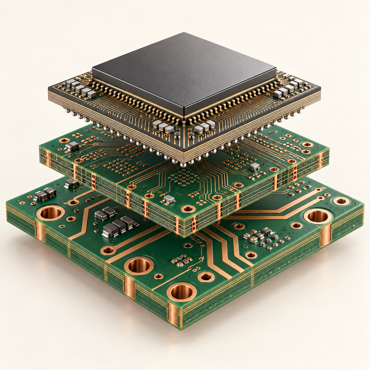
A PCB supports system-level connections; HDI technology increases routing density with finer features and microvias; an IC substrate sits between the chip and the system PCB.
AI hardware is supporting demand for high-layer-count PCBs, HDI structures, IC substrates, and advanced packaging materials, but each category benefits at a different point in the value chain.
High-layer-count PCBs are widely used in server boards, switches, backplanes, and midplanes, while IC substrates are more directly associated with the packaging of GPUs, CPUs, AI accelerators, and other high-compute chips.
As board thickness, connection density, and hole complexity increase, PCB copper plating requires tighter control of copper distribution, bath chemistry, and raw-material consistency.
Discussions of AI servers, GPUs, and advanced packaging often use the terms PCB, HDI, IC substrate, and package substrate in the same conversation.
They all belong to the electronics manufacturing ecosystem, but they are not the same thing.
A PCB is the most common interconnection platform in an electronic system. HDI is a set of technologies used to increase PCB routing density. An IC substrate is closer to the chip itself and provides a critical connection layer between a semiconductor package and the system PCB.
Understanding the difference helps clarify where AI-driven demand is actually occurring across the electronics supply chain.
1. What Is a PCB?
PCB stands for printed circuit board.
Its essential role is to:
provide mechanical support, electrical interconnection, power distribution, ground references, and signal paths for electronic components.
A typical PCB contains insulating materials, patterned copper layers, vias, solder mask, and surface finishes.
PCBs are used in a wide range of products, including:
consumer electronics;
industrial controls;
automotive electronics;
communications equipment;
servers;
network switches;
medical equipment; and
power systems.
An AI server contains much more than one main board. A complete system may use server motherboards, GPU or accelerator boards, switch boards, power boards, backplanes, midplanes, storage-module boards, and control boards.
2. What Is HDI?
HDI stands for high-density interconnect.
HDI does not simply mean “a PCB with more layers.” It refers to PCB technologies that achieve greater routing density in a limited area through finer lines, smaller holes, and more complex interlayer connections.
HDI construction may include:
laser-drilled microvias;
blind vias;
buried vias;
stacked microvias;
finer line and space;
thinner dielectric layers;
sequential lamination or build-up structures; and
tighter registration control.
A useful way to understand HDI is:
When conventional through holes and normal routing can no longer accommodate the required connections, HDI increases capability by making those connections smaller, denser, and more precise.
HDI is widely used in smartphones, wearables, automotive electronics, communications modules, premium consumer devices, and certain high-performance computing products.
In AI hardware, it may appear in high-I/O-density modules, compact systems, or areas requiring complex local interconnection. Not every AI-server PCB, however, uses the same HDI structure.
3. What Is an IC Substrate?
An IC substrate is also called a package substrate.
It sits between the semiconductor die or package and the system PCB, making it a critical part of advanced packaging.
The relationship can be simplified as:
Chip
↓
IC substrate
↓
PCB
↓
Server, switch, or other electronic system
Connections on a chip are extremely fine, while connections on a system PCB are comparatively larger. The IC substrate redistributes signals, power, and ground between these different connection scales.
It commonly requires:
finer lines and spaces;
smaller microvias;
higher interconnection density;
tighter dimensional stability;
better flatness;
demanding package-reliability performance; and
more precise materials and fabrication control.
Substrates for high-performance computing, GPUs, CPUs, networking chips, and AI accelerators may face especially demanding requirements for size, routing density, warpage, thermal management, and reliability.
An IC substrate can look similar to a circuit board, but its manufacturing logic, precision requirements, and position in the product architecture differ substantially from those of a conventional system-level PCB.
4. PCB vs. HDI vs. IC Substrate
ComparisonPCBHDIIC SubstratePrimary roleConnect components and system modulesIncrease PCB routing densityConnect a chip package to the system PCBConnection levelSystem levelSystem or module levelChip-package levelTypical featuresThrough holes, blind vias, buried viasMicrovias, blind vias, build-up structuresMicrovias, ultra-fine traces, high-density package interconnectsTypical applicationsServers, switches, industrial equipmentPhones, communications modules, selected high-end compute modulesGPUs, CPUs, AI chips, advanced packagesManufacturing focusLayer count, thickness, through-hole copper, impedance, reliabilityMicrovia reliability, fine features, registrationUltra-fine circuitry, package reliability, warpage, dimensional controlAI relevanceSupports server and network systemsSupports dense modules and local interconnectsDirectly supports high-performance chip packaging
These categories are not a simple “low-end to high-end” hierarchy. They address different locations, structures, and functions in an electronic system.
One AI server may use high-layer-count PCBs, HDI features, and IC substrates at the same time.
5. Which Category Is Growing Faster in the AI Era?
There is no single answer because AI demand spans chips, packages, servers, network equipment, data centers, and power systems.
1. IC Substrates: Driven by High-Performance Chips and Advanced Packaging
AI training and inference require more capable GPUs, CPUs, AI accelerators, and network processors.
Larger package sizes, higher I/O counts, greater power density, and higher bandwidth requirements make advanced IC substrates an important part of the packaging chain.
Demand is closely connected to:
shipments of high-performance GPUs;
new AI-accelerator platforms;
packaging for high-bandwidth memory;
larger packages and chiplet architectures; and
advanced-packaging capacity and yield.
2. High-Layer-Count PCBs: Driven by AI Servers and Networking Equipment
High-layer-count PCBs are used in AI-server motherboards, switches, backplanes, midplanes, and rack-scale interconnect systems.
As GPU count, network bandwidth, and power requirements increase, system-level PCBs may need to carry more high-speed signals, power, ground, and control functions.
This can increase demand for:
higher layer counts;
larger board formats;
more complex stackups;
higher-aspect-ratio through holes;
tighter impedance control;
more uniform in-hole copper plating; and
stronger reliability performance.
For this reason, high-layer-count PCBs are among the system-level components most directly affected by AI infrastructure expansion.
3. HDI: Driven by Density, Miniaturization, and Complex Module Design
HDI growth is not driven by AI alone. Smartphones, automotive electronics, communications equipment, wearables, and industrial products also depend on high-density interconnect technology.
Within AI hardware, HDI may benefit from dense modules, network equipment, edge-AI products, and selected accelerator-related designs.
Its central value is straightforward:
Fit more connections into a smaller area while reducing signal path length and packaging pressure.
6. Why Does AI Hardware Make PCB Manufacturing More Difficult?
An AI server is not simply a computer with more GPUs.
It must manage high-speed signals, high-current power delivery, thermal control, storage, control functions, and networking within a limited space.
This creates several manufacturing challenges:
more layers and greater board thickness;
higher through-hole aspect ratios;
greater sensitivity to impedance and signal loss;
more complex power and ground structures;
tighter requirements for in-hole copper uniformity;
more demanding thermal-cycle reliability; and
greater importance of lot-to-lot process consistency.
As boards become thicker and holes become deeper or smaller, it becomes more difficult for plating solution to reach the hole center and build a uniform copper layer.
Advanced PCB competition is therefore not only about materials and design. It also depends on drilling, electroless copper, electroplating, lamination, inspection, and quality traceability.
7. What Does This Have to Do with Electronic-Grade Copper Oxide?
Electronic-grade copper oxide is not a final component of a GPU, an IC substrate, or a finished PCB.
Its role can arise in certain insoluble-anode acid copper-plating systems used during PCB manufacturing.
In such a system, copper ions are continuously deposited onto PCB surfaces and hole walls, so Cu²⁺ must be replenished from an external source.
Electronic-grade copper oxide can react under acidic conditions to provide Cu²⁺ as one replenishment material.
For a complex PCB plating system, buyers commonly need to assess:
metallic impurities;
chloride and other ionic residues;
acid-insoluble matter;
sulfuric-acid dissolution time;
dissolution behavior in the actual plating bath;
particle size and flowability;
consistency across consecutive lots; and
COA documentation and traceability.
Growing AI demand for advanced PCBs does not mean that any product labeled “electronic grade” will be suitable.
What matters is whether the material performs consistently in the customer’s actual process and supports controlled, continuous copper plating.
Conclusion
PCB, HDI, and IC substrates may all resemble circuit boards, but they operate at different levels of the electronics ecosystem: system interconnection, dense module interconnection, and chip-package interconnection.
The AI era is not increasing demand for only one category. It is upgrading the entire manufacturing chain:
More capable chips require more advanced package substrates.
Larger server systems require more complex high-layer-count PCBs.
Denser modules require HDI technology.
More demanding PCB structures require stable copper plating and consistent electronic materials.
For electronic-material suppliers, understanding this chain is more useful than applying a generic “AI material” label.
FAQ
Are PCB, HDI, and IC substrates the same product?
No. PCBs mainly provide system-level interconnection, HDI is a group of technologies for increasing PCB routing density, and IC substrates connect the chip package to the system PCB.
Does HDI always have more layers than a standard PCB?
No. HDI is defined by high-density features such as microvias, fine lines, build-up construction, and precise interlayer connections—not simply by layer count.
Is an IC substrate a type of PCB?
IC substrates and PCBs share certain materials and manufacturing concepts, but substrates serve package-level interconnection and generally require greater precision, dimensional stability, and reliability control. They are usually discussed as a separate package-substrate category.
What types of boards are used in an AI server?
An AI server may use high-layer-count PCBs, HDI features, backplanes, midplanes, power boards, and module boards. The exact combination depends on the computing platform, network architecture, cooling approach, and equipment design.
Why are AI-server PCBs harder to plate?
Greater layer count and board thickness can increase through-hole aspect ratio. Solution exchange and current distribution are weaker near the center of a deep hole, which can lead to thin center-wall copper or uneven thickness if the process is not well controlled.
Is electronic-grade copper oxide used directly in AI chips?
No. Certain electronic-grade copper oxide products can be used as an external Cu²⁺ source in insoluble-anode acid copper-plating systems. Their role occurs during PCB manufacturing, not inside the finished chip.
This article was prepared by the Zhongan Copper technical team.
Zhongan Copper develops and manufactures high-purity active copper oxide powder for electronic applications, including insoluble-anode acid copper-plating systems used in PCB, FPC, and HDI production.
Contact our technical team to request product specifications, a lot COA, particle-size data, sulfuric-acid dissolution results, plating-bath dissolution data, or sample-validation support.
Final product specifications and application results are subject to the COA for the delivered lot, the agreed test method, and validation in the customer’s production process.